ALU design
I. Introduction
In this lab you are basically building a 2-bit ALU. You are required to
write a behavioral description of an ALU. Note: when constructing the
ALU, do not use LE's, AE's, and FA's as shown in the book. All you
really need are case statements, etc ... The ALU should take in two
2-bit numbers and have the following functionality:
- Add the numbers
- Subtract the numbers
- NOR the numbers
- NAND the numbers
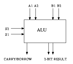
The output of the ALU will consist of one 2-bit result and a
carry/borrow bit. You are also required to write a testbench for
this design. You will have to feed values into your design and
demonstrate that it is correct by simulating your desgin using
ALDEC Active-VHDL (using the testbench you wrote) and then
downloading the design unto an XS40 board.
II. Procedure
Implementing and simulating the design
- Run Active VHDL by clicking on the icon on the desktop.
If a window pops up regarding evaluation terms, click
on "I Agree"
- Create a new design and store in in C:\temp
- Select "Add existing resource files" if you have already typed
up your vhdl, otherwise select "Create new source files now"
- Once you have gotten you files loaded and compiled into Active
VHDL, select Simulation->Initialize Simulation. (If you
do not remember how to load and compile files go back to
the Aldec tutorial)
- Click on the small button next to the save icon to create a new
waveform.
- Select "Waveform->Add Signals" and add all the signals in your
testbench.
- Push the "Run" button and see if the output is what you hoped it
would be.
Download VHDL
- After you have verified the results using ALDEC, check out an
XS40 board from the T.A. to download your code and verify
your results.
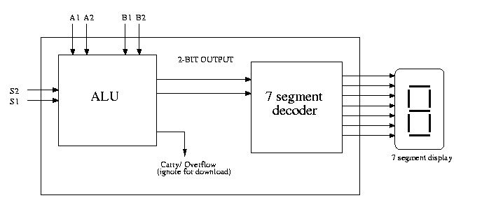
- To view the results of your ALU on the XS40 board, you
will need to connect the ALU to the decoder you previously
designed. Below is a schematic showing how this could
be done.
- There are several things you should keep in
mind when modifying your code for download:
- The ALU outputs a 2-bit number, the 7-segment
decoder takes a 4-bit number as intput. This
needs to be remedied when connecting the two
components.
- You should ignore the carry/overflow bit when
downloading
- A .ucf file needs to be created so that the inputs
and outputs of your design are connected
to the desired pins, you can look at previous
.ucf files to get an idea of how this might
be done.
- Load your modified design into Xilinx and generate a
bit file (if you do not remember how to do this
go back to the Xlinix synthesis tutorial).
- Load your bit file onto to the XS40 board and test
your ALU.