Interfacing: Converting 8-bit LCD communication to 4-bit
Introduction
One of the challenges an embedded systems designer must face is the limited number of output pins on a microprocessor, in the case of the 8051 we are limited to 32. If we have a large number of peripherals connected to the 8051 we might not have the luxury of using 8 pins to interface to the LCD. The Optrex LCD has two modes, an 8-bit interface and a 4-bit interface. In this lab we will implement the 4-bit LCD interface.
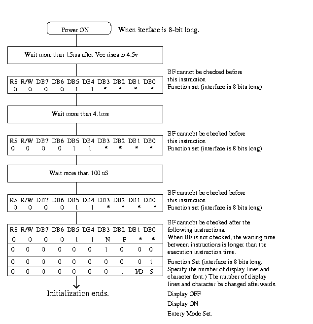
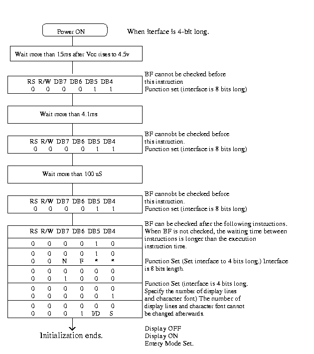
Before an LCD can be used it must be initialized. Both the 8-bit and 4-bit initialization sequence is listed below. The following figures provide the contents of the Optrex databook for the LCD. You can also print these out here 8-bit interface 4-bit interface.
|
|
| Instruction | Code | Description | Execution Time (max.) fosc=250KHz | |||||||||
| RS | R/W | DB7 | DB6 | DB5 | DB4 | DB3 | DB2 | DB1 | DB0 | |||
| Clear Display | 0 | 0 | 0 | 0 | 0 | 0 | 0 | 0 | 0 | 1 | Clears all display and returns the cursor to the home position (Address 0). | 1.64 mS |
| Cursor At Home | 0 | 0 | 0 | 0 | 0 | 0 | 0 | 0 | 1 | * | Returns the cursor to the home position (Address 0). Also returns the display being shifted to the original position DDAM contents remain unchanged. | 1.64 mS |
| Entry Mode Set | 0 | 0 | 0 | 0 | 0 | 0 | 0 | 1 | I/D | S | Sets the cursor move direction and specifies or not to shift the display. These operations are performed during data write and read. | 40 µS |
| Display On/Off Control | 0 | 0 | 0 | 0 | 0 | 0 | 1 | D | C | B | Sets ON/OFF of all display (D) cursor ON/OFF (C), and blink of cursor position character (B). | 40 µS |
| Cursor/Display Shift | 0 | 0 | 0 | 0 | 0 | 1 | S/C | R/L | * | * | Moves the cursor and shifts the display without changing DDRAM contents. | 40 µS |
| Function Set | 0 | 0 | 0 | 0 | 1 | DL | N | F | * | * | Sets interface data length (DL), number of display lines (N) and character font (F). | 40 µS |
| CGRAM Address Set | 0 | 0 | 0 | 1 | ACG | Sets the CGRAM, data is sent and received after this setting. | 40 µS | |||||
| DDRAM Address Set | 0 | 0 | 1 | ADD | Sets the CGRAM, data is sent and recived after this setting. | 40 µS | ||||||
| Busy Flag/Address Read | 0 | 1 | BF | AC | Reads Busy flag (FB) indicating internal operation is being performed and reads address counter contents. | 0 µS | ||||||
| CGRAM/DDRAM Data Write | 1 | 0 | WRITE DATA | Writes data into DDRAM or CGRAM. | 40 µS | |||||||
| CGRAM/DDRAM Data Read | 1 | 1 | READ DATA | Reads data into DDRAM or CGRAM. | 40 µS | |||||||
| Code | Description | Executed Time(max.) | ||||||||||||||||
|
DDRAM: Display Data RAM CGRAM: Character Generator RAM ACG: GCRAM Address ADD: DDRAM Address Corresponds to cursor address. AC: Address Counter, used for both DDRAM and CGRAM *: Invalid |
fcp or fosc=250kHz However, when frequency changes, execution time also changes Ex If fcp or fosc is 250kHz, 37µS x (270/250)=40µS |
Assignment
Appartus Required
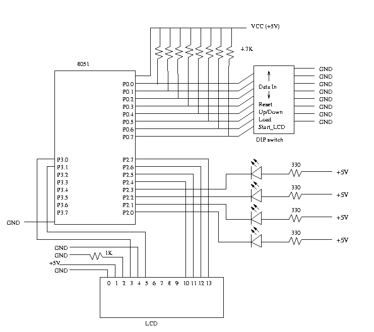
Schematic
Procedure
P2 = 0;
The four LED's connected to the
lower 4 bits of P2 should always remain on. You must ensure
that the lower 4 bits of P2 do
not change, as these pins may be necessary to control
other aspects of an embedded system. Thus, if your
modifications are correct, the LCD should function
properly and the LED's should not blink.