Introduction to FPGAs using VHDL
I. Introduction
In the previous lab Xilinx was used to graphically draw the
circuit by connecting a series of AND gates and OR gates.
In this lab you will be taking the previously constructed
circuit and describe it in VHDL. To do this you will need to
construct entities which mimic the gates used. Then
connect the "gates" to construct the 7 segment decoder.
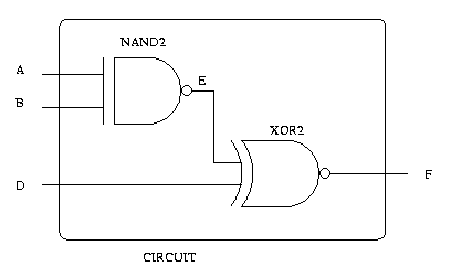
Suppose we want to construct the above circuit.
First we have to construct entities which act as NAND2 and XOR2 gates.
Then we would plug our input values into these entities to get our result.
An example of this may be as follows:
...

-- first we want to declare the structure of the entity
-- (i.e. the number of inputs and outputs to the entity)

entity NAND2 is
   port ( input1, input2: in STD_LOGIC;
          output1: out STD_LOGIC
        );
end NAND2;

-- then we describe the internal behavior of the entity
-- (i.e. what the entitiy does to the inputs to ge the output)

architecture beh_nand2 of NAND2 is
begin
   output1 <= input1 nand input2;
end beh_nand2;


-- we do the same for the X0R2 gate

entity XOR2 is
   port ( input1, input2: in STD_LOGIC;
	  output1: out STD_LOGIC
        );
end OR2;

architecture beh_xor2 of XOR2 is
begin
   output1 <= input1 xor input2;
end beh_xor2;


-- now we declare CIRCUIT's structure
-- (i.e. the number of inputs and output to the entity)

entity CIRCUIT is
   port ( a, b, c : in STD_LOGIC;
          f: out STD_LOGIC;
        );
end CIRCUIT;

-- the internal behvaior is describe here

architecture struct of CIRCUIT is

-- a signal has two purposes, as a wire or register
-- in our example we use it as a wire whose purpose is
-- to connect two components together (as seen in the above image)

signal e: STD_LOGIC;

-- we want to use the previously constructed gates so
-- we declare them as components in our entity

component NAND2
   port ( input1, input2: in STD_LOGIC;
          output1: out STD_LOGIC
        );
end component;

component XOR2
   port ( input1, input2: in STD_LOGIC;
          output1: out STD_LOGIC
        );
end component;

-- then we describe how the inputs and outputs of CIRCUIT
-- are fed through the gates previously described

begin
   X1: NAND2 port map(A, B, E);
   X2: XOR2 port map(E, D, F);

end struct;

...
II. Implementation
- Start up Xilinx and select "Create a New Project" Save it in temp
as before. Name it decoder and select the "HDL" instead of the
"Schematic Capture" option. Click OK.
- Click on the little paper icon in the "Design Entry" button.
This should bring up the HDL editor. Choose "Create Empty".
Click OK.
- Write all of the code to structurally implement the design from
the previous lab. The schematic should translate directly into
this design only now you should have entities for each component, like
an entity for a three input OR gate and others.
- Once you have all the program typed in go to "Synthesis" and select
"Check Syntax". After ensuring that there are no syntax errors,
go back to the "Project Manager".
- Now you need to add your design to the project. Go to
"Document" and click on "Add". Select your document and
click OK.
- Select the "Synthesis" step as the next step in the design
process. Ensure that the "BCD" entity that you created
is selected for the "Top Level" (i.e. in our example we
created a NAND gate and an XOR gate, but CIRCUIT is the top
level entity), and that the Target Device information is as follows:
"Family" = XC4000XL, "Device" = 4010XLPC84. Now click on "Run".
- Now verify the correctness of your VHDL code, by selecting the
"Simulation" button. Add the appropriate signals to your waveform, and
their stimuli as you did in the previous laboratory assignment.
III. Downloading
- Go back to the "Project Manager" and replace
"decoder.ucf" with this
file.
- Click on the "Implementation" button.
- Click on "Run". It should go through a series of
steps. In the end it should say "Implementation
Sucsess". If this is not the case, check the error
log for problems.
- Open a "Command Prompt" terminal and cd to
"c:\temp\decoder".
- Make sure your XS40 board is powered up, connected to
the computer, and that all the switches on the DIP switch
are connected to ground (if any are high your program
will not load properly).
- Type "xsload decoder.bit" on the prompt and hit
"enter".
- The DIP switches are your input signals. Toggle the
DIP switch and see if the number on the LED corresponds
to the inputs correctly (i.e. if your DIP switch is
"1111" you should see "F" on the LED).