FSM Design: Parallel to Serial Convertor
I. Introduction
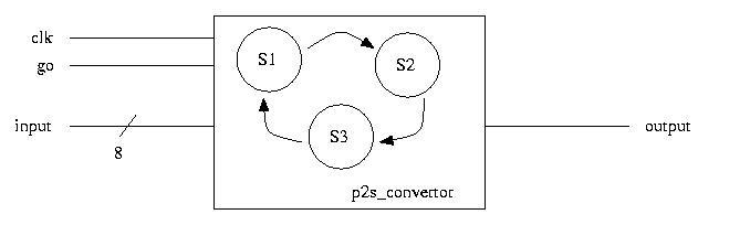
For this lab, you are required to write an FSMD vhdl description of a parallel to serial converter and a testbench to show its correctness.
The FSMD must be of your own design. The following are the inputs and outputs expected of your design:
Your parallel to serial convertor works as follows. The machine should wait until the 'go' signal becomes active (high) and then transmit the data using the following protocol: The output should be kept high until it is going to send information on it. You must then send a start bit ('0') followed by the data going from high order to low order followed by a stop bit ('1'). There should be one bit transmitted per clock cycle. NOTE: The go signal should not be treated as an enable. It is simply used to tell your machine when to begin transmitting data.
II. Procedure
III. Downloading(?)