Intro to FPGA's with schematic capture
I. Introduction
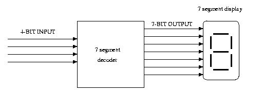
The purpose of this lab is to design a 7 segment decoder. Your circuit
will read in a 4-bit binary value (in1 throught in4) and output 7
signals (a through g) which will then light up the appropriate leds on
the 7 segment display. For example, if you input 1000, you would expect
to see an 8 on the display. If your circuit is working properly then
all 7 outputs on the led should be high (illuminated).
II. Procedure
creating the decoder
- Click on the Xilinx Foundation Software Icon on the desktop.
The "Getting Started" window should pop up. Select the "Create
a new project" option and then click on "OK".
- Enter "lab1" as the project name, and change the directory
name to "C:\temp". Select "XC4000XL", family for the FPGA,
from the first drop-down menu at the bottom. And Select the
"4010XLPC84", for the component number, from the second drop-down
menu at the bottom. Ensure that the "Schematic" option is
selected for the "flow" option. Click on "OK".
- Click on the Schematic Editor in the Design Entry stage
(Icon shaped like a gate) A new shematic editor window should
now appear. Click on "Mode", and select "Symbols". A symbol
window list should now pop up.
The following truth table represents the functionality of a
7-segment decoder that you are designing:
        g
       ---
     f| d |e
       ---
     c|   |b
       ---
        a
| IN1 |
IN2 |
IN3 |
IN4 |
|
a |
b |
c |
d |
e |
f |
g |
| 0 |
0 |
0 |
0 |
|
1 |
1 |
1 |
0 |
1 |
1 |
1 |
| 0 |
0 |
0 |
1 |
|
0 |
1 |
0 |
0 |
1 |
0 |
0 |
| 0 |
0 |
1 |
0 |
|
1 |
0 |
1 |
1 |
1 |
0 |
1 |
| 0 |
0 |
1 |
1 |
|
1 |
1 |
0 |
1 |
1 |
0 |
1 |
| 0 |
1 |
0 |
0 |
|
0 |
1 |
0 |
1 |
1 |
1 |
0 |
| 0 |
1 |
0 |
1 |
|
1 |
1 |
0 |
1 |
0 |
1 |
1 |
| 0 |
1 |
1 |
0 |
|
1 |
1 |
1 |
1 |
0 |
1 |
1 |
| 0 |
1 |
1 |
1 |
|
0 |
1 |
0 |
0 |
1 |
0 |
1 |
| 1 |
0 |
0 |
0 |
|
1 |
1 |
1 |
1 |
1 |
1 |
1 |
| 1 |
0 |
0 |
1 |
|
0 |
1 |
0 |
1 |
1 |
1 |
1 |
| 1 |
0 |
1 |
0 |
|
0 |
1 |
1 |
1 |
1 |
1 |
1 |
| 1 |
0 |
1 |
1 |
|
1 |
1 |
1 |
1 |
0 |
1 |
0 |
| 1 |
1 |
0 |
0 |
|
1 |
0 |
1 |
0 |
0 |
1 |
1 |
| 1 |
1 |
0 |
1 |
|
1 |
1 |
1 |
1 |
1 |
0 |
0 |
| 1 |
1 |
1 |
0 |
|
1 |
0 |
1 |
1 |
0 |
1 |
1 |
| 1 |
1 |
1 |
1 |
|
0 |
0 |
1 |
1 |
0 |
1 |
1 |
- The next step is to generate the minimized equations for the
outputs "a" through "g" using the Karnaugh map.
- Now that you have equations for the outputs "a" through "g", you
must draw the schematic which must eventually be downloaded on
to the XS40 board.
- Click on the "Hierarchy Connector", which should result in a
new pop-up window. In this window, for the inputs select
"Input" for the "Terminal Type", and enter the appropriate
terminal names ("IN1" through "IN4"). Select the "IBUF" for all
of the four inputs from the symbol table, and connect each input
to an "IBUF". Now generate the rest of the circuit according to
your minimized equations.
- Now Generate the outputs using the "Hierarchy Connector" as done
in step 10, and do not forget to add the necessary "OBUF" before
the output pads.
simulating and verifying the design
- We are now ready for simulation. Save the file in your project
directory, make sure that the filename is less than 5 characters
in length, and then select "Options", and choose "Create
Netlists". Following that, choose "Integrity Check" and finally
select "Export Netlists". A window will pop-up at this point,
select "Edit 200 [*.EDN]" in the "Files of Type" selection box.
Now click on "Open", and the netlist will be exported. Select the
"File" drop-down menu, and exit the schematic editor. Make
"lab1.sch" a part of the schematic by selecting the
"Document" drop-down menu, and click on "Add" to add your
schematic to the list of schematics in the project. Now click on
"Simulation" This will bring up the waveform viewer. At this
point go to "Signal", and click on "Add Signals". Add only the
input signals, and the output signals that you created in your
schematic.
- Now we need to apply simulators to the input signals to have
interesting things happen to our output signals. Select the
"Signal" drop-down menu, and select "Add Simulators" menu item.
We are interested in the binary counter stimulus labeled "BC".
Select the appropriate bits corresponding to the inputs in your
design (ex: the LSB - least significant bit, should be connected
to the least significant bit in your inputs). This is
accomplished by selecting the input signal followed by the
appropriate stimulus.
- Once all of the inputs have been mapped, we need to set up a
parameter that controls the speed of the simulation. Select the
"options" drop-down menu followed by the "Preferences" menu item.
Then in the preferences window set the appropriate values for the
"B0 Period" and the "Simulation Precision" to obtain an easily
viewable waveform.
- Now select "Options" -> "Long Simulation" and enter the
time-period for your simulation (eg: 2 seconds). After insuring
the correctness of your output, contact either a TA or lab
assistant to be checked-off for this portion of the laboratory
assignment.
II. Downloading
Creating a bitstream
- You must now modify your schematic by replacing
all of your input and output signals so that they
may be mapped to the appropriate pins on the XS40
board. Replace all of the hierarch connectors with
"IPADS", which will be connected to the "IBUF"
symbols.
- You will have to map the pins on the board to these
pads. To do this, select each pad and double click
on it. This should bring up a window labeled "Symbol
Properites." In this window type "LOC" into the "Name"
box and in the "Description" box type in the pin number
to the corresponding input:
- IN1 - p80
- IN2 - p81
- IN3 - p10
- IN4 - p14
For each input lick the "Add" button and then
"OK" each time.
- Follow the same steps for the output pads, but label
the descriptions as follows:
- a - p19
- b - p18
- c - p23
- d - p20
- e - p24
- f - p26
- g - p25
- Save this to a different file name and return to the
"Project Manager" (the originial window that opened).
Add this new file to the project
- Click on the Implementation button. This should bring
up the "Implementation Design" window. Select
"4010XLPC84" in the "Device" box. Click on "Run".
downloading the bitstream file unto the XS40 board
- Open a "Command Prompt" terminal and cd to
"c:temp\lab1".
- Make sure your XS40 board is powered up, connected
to the computer, and that all the switches on the
DIP switch are connected to ground (if any are high
your program will not load properly).
- Type "xsload lab1.bit" on the prompt and hit
"enter".
- The DIP switch are your input signals. Toggle the
DIP switch and see if the number on the LED corresponds
to the input (i.e. if your DIP switch is "1111" you
should see "F" on the LED).