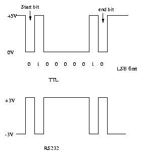
Fig 1. Serial Waveforms
Serial Communication
Introduction
To establish a serial communication link between the PC and the 8051.
Serial communication is often used either to control or to receive data from an embedded microprocessor. Serial communication is a form of I/O in which the bits of a byte begin transferred appear one after the other in a timed sequence on a single wire. Serial communication has become the standard for intercomputer communication. In this lab, we'll try to build a serial link between 8051 and PC using RS232.
RS232C:
The example serial waveforms in Fig 1 show the waveform on a
single conductor to transmit a byte (0x41) serially. The upper waveform
is the TTL-level waveform seen at the transmit pin of 8051. The lower
waveform shows the same waveform converted to RS232C levels. The voltage
level of the RS232C are used to assure error-free transmission over greater
distances than would be possible with TTL levels.
As shown in Fig 1, each byte is preceded by a start bit and followed
by one stop bit. The start and stop bits are used to synchronize the
serial recivers. The data byte is always transmitted
least-significant-bit first. For error checking it is possible to
include a parity bit as well, just prior to the stop bit. The bits are
transmitted at specific time intervals determined by the baud rate
of the serial signal. The baud rate is the reciprocal of the time to send
1 bit. Error-free serial communication requires that the baud rate, number
of data bits, number of stop bits, and presence or absence of a parity bit
be the same at the transmitter and at the receiver.
Fig 1. Serial Waveforms
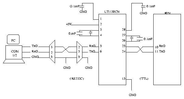
Using the Serial Port:
8051 provides a transmit channel and a receive channel of serial
communication. The transmit data pin (TXD) is specified at P3.1,
and the receive data pin (RXD) is at P3.0. The serial signals provided
on these pins are TTL signal levels and must be boosted and
inverted through a suitable converter(LT1130CN is used in this lab)
to comply with RS232 standard.
All modes are controlled through SCON, the Serial CONtrol register.
The SCON bits are defined as SM0, SM1, SM2, REN, TB8, RB8, TI, RI
from MSB to LSB. The timers are controlled using TMOD, the Timer MODe
register, and TCON, the Timer CONtrol register.
Register Descriptions:
          SCON bit definitions

          SCON Serial Control Register

         (msb)                      (lsb)
          -----------------------------
         |SMO|SM1|SM2|REN|TB8|RB8|TI|RI|
          -----------------------------

         SMO, SM1, SM2 Serial Mode COntrol Bits

         SM0 SM1  Mode Baud Rate
         -----------------------
          0   0    0    fosc/12
          0   1    1    variable
          1   0    2    fosc/32 or fosc/64


        SM2  Multiprocessor Mode Control Bit

        1 = Multi-processor mode
        0 = Normal mode

        REN Receiver Enable Bit

        1 = Receive Enable
        0 = Receive Disabled

        TB8 9th Transmit Bit
            Enabled only in modes 2 and 3

        RB8 9th Bit Received
            Used in modes 2 and 3

        RI, TI Serial Interrrupts

            RI is set to indicate receipt of a serial word and TI
            is set to indicate completion of a serial transmission.


-----------------------------------------------------------------------------


       TMOD Timer Mode Register

       ------------------------------
      |Gate|C/T|M1|M0|Gate|C/T\|M1|M0|
       ------------------------------
      |<-Timer 1----><---Timer 0 --->

      Gate Gating Control.
           0= Timer enabled
           1 = Timer enabled if INTx\ is high

      C/T\ Counter or Timer Selector
           0 = Internal count source (clock/12)
           1 = External count source (Tx pin)

      M1, M0 Mode Control
          M1 M0          Mode
          ----------------------------------
          0   0    Mode 0, 13 bit count mode
          0   1    Mode 1, 16 bit count mode
          1   0    Mode 2, Auto reload mode
          1   1    Mode 3, Multiple mode

-----------------------------------------------------------------------------

        TCON Timer Control Receiver Register

        ---------------------------
       |TF1|TR1|TF0|TR0|  |  |  |  |
        ---------------------------
       <-Timer Controls><-Unused for timers

        TRx Timer x run control
            0 = Timer not running
            1 = Timer running

        TFx Timer x flag
            0 = timer has not rolled over
            1 = timer has rolled over

----------------------------------------------------------------------------

     Formula to load the value of TH1 corresponding to required baud rate

          Clock Frequency (12 MHz)
          -----------------------  = Baud Rate
          12 x 32 x (256-TH1)
RS232 connector:
PCs have 9pin/25pin male SUB-D connectors. The pin layout is as follows
(seen from outside your PC):
        1                         13         1         5
      _______________________________      _______________
      \  . . . . . . . . . . . . .  /      \  . . . . .  /
       \  . . . . . . . . . . . .  /        \  . . . .  /
        ---------------------------          -----------
        14                       25           6       9

 Name (V24)  25pin  9pin  Dir  Full name               Remarks
--------------------------------------------------------------------------
    TxD         2     3    o   Transmit Data
    RxD         3     2    i   Receive Data
    RTS         4     7    o   Request To Send
    CTS         5     8    i   Clear To Send
    DTR        20     4    o   Data Terminal Ready
    DSR         6     6    i   Data Set Ready
    RI         22     9    i   Ring Indicator
    DCD         8     1    i   Data Carrier Detect
    GND         7     5    -   Signal ground
     -          1     -    -   Protective ground       Don't use this one
                                                       for signal ground!
The most important lines are RxD, TxD, and GND. Others are used with
modems, printers and plotters to indicate internal states.
In this lab, we are going to use
serial.exe, to communicate between the PC and the 8051.
Assignment:
Apparatus Required:
Schematic:
Program:
#pragma SMALL DB OE
#include <reg51.h>

unsigned char ReceiveSerial() {

	unsigned char c;

	TMOD = 0x20;	/* configure timer for the correct baud rate */
        TH1 = 0xe6;     /* 1200 bps for 12 MHz clock */
        TCON = 0x00;    /* Set timer to not running */

	SCON = 0x50;    /* Set Serial IO to receive and normal mode */
	TR1 = 1;	/* start timer to Receive */
	while( (SCON & 0x01) == 0 ) /* wait for receive data */;
	c = SBUF;
	return c;
}

void SendSerial(unsigned char c) {

        /* initialize..set values for TMOD, TH1 and TCON */
        /* set the Tx interrupt in SCON to indicate sending data */
        /* start timer */
        /* write character to SBUF */
        /* wait for completion of sent data */
}

void main(void) {

	unsigned char c;

	while( 1 ) {

           /* Use ReceiveSerial to read in a character 'c' */
           /* Do some computation on 'c' */
           /* Send the result using SendSerial() */
        }
}
Procedure: