Introduction to VHDL Simulation and Synthesis:
Blinking LEDs Lab

I. Introduction
The purpose of this lab is to introduce you to VHDL simulation and
synthesis using the ALDEC VHDL simulator and the Xilinx foundation
software for synthesis. There are several defenitions that may be
helpful:
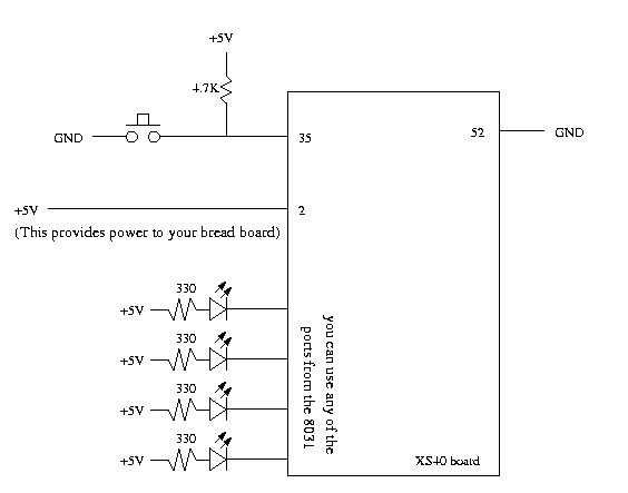
In this lab, you will implement a behavioral description of a 2-bit counter (00, 01, 10, 11, 00, ...). The counter's output is fed to a 2-4 decoder. This decoder's output is the output of the top level entity (see picutre above). The output of the top level entity is then fed to four led's. The leds should correspond as follows:
| counter output | L0 | L1 | L2 | L3 |
|---|---|---|---|---|
| reset | 0 | 0 | 0 | 0 |
| 00 | 0 | 0 | 0 | 1 |
| 01 | 0 | 0 | 1 | 0 |
| 10 | 0 | 1 | 0 | 0 |
| 11 | 1 | 0 | 0 | 0 |
The counter and decoder should be written behaviorally. A
behavioral style architecture specifies what a
particular system does but provides no information on how the
design is implemented (i.e. don't use AND, OR, NAND, ... gates
to implement your design). In this lab, you will specify an
entity and test it, synthesize your design using FPGA Express
and download it onto an XS40 board using the Xilinx Foundation
software.
III. Schematic:
On the XS40 board:
No power supply is needed for this lab, you can think of
pins 2 and 52 as on "onboard power supply." In addition the
button is used as the clock signal. The onboard clk is 12MHz, this
is too fast for us to see the lights blink. Instead of using
a clock divider to slow down the signal, we create our own clock
signal using the button (Don't forget to change your .ucf file
to represent our pseudo clock).

II. Procedure:
simulation
synthesis