Synthesis:
Behavioral description of a 7-segment decoder
I. Introduction
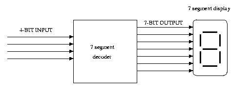
In previous labs, a structural description of a 7-segment decoder
was written. The purpose of this lab is to re-write the code
so that the 7-segment decoder is described behaviorally. To do
this a distinction must be made between a behavioral description
and a structural description.
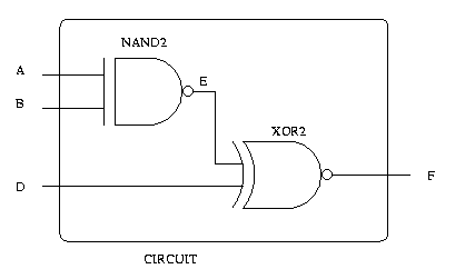
Suppose we want to construct the above circuit. We can describe the
circuit in several ways.
STRUCTURAL DESCRIPTION
If we were to describe the above circuit structurally we would first
have to construct entities which act as AND2 and OR2 gates. Then we
would plug our input values into these entities to get our result. This
was done in the
Introduction to FPGAs using VHDL lab, the example given was as follows:
...

entity NAND2 is
   port ( input1, input2: in STD_LOGIC;
          output1: out STD_LOGIC
        );
end NAND2;

architecture beh_nand2 of nAND2 is
begin
   output1 <= input1 nand input2;
end beh_nand2;


entity XOR2 is
   port ( input1, input2: in STD_LOGIC;
	  output1: out STD_LOGIC
        );
end XOR2;

architecture beh_xor2 of XOR2 is
begin
   output1 <= input1 xor input2;
end beh_xor2;


entity CIRCUIT is
   port ( a, b, c : in STD_LOGIC;
          f: out STD_LOGIC;
        );
end CIRCUIT;

architecture struct of CIRCUIT is

signal e: STD_LOGIC;

component NAND2
   port ( input1, input2: in STD_LOGIC;
          output1: out STD_LOGIC
        );
end component;

component XOR2
   port ( input1, input2: in STD_LOGIC;
          output1: out STD_LOGIC
        );
end component;

begin
   X1: NAND2 port map(A, B, E);
   X2: XOR2 port map(E, D, F);

end struct;

...
BEHAVIORAL DESCRIPTION
If we were to describe the above circuit behaviorally we would not have
to worry about mimicing the gates. Instead we can describe the result
at a more abstract level which greatly simplifies things as seen below:
...

entity CIRCUIT is
   port ( a, b, d: in STD_LOGIC;
	  f: out STD_LOGIC
        );
end CIRCUIT;

architecture beh of CIRCUIT is
begin
   f <= (a nand b) xor d;
end beh;

...
II. Procedure
Implement the entity
- Start up Xilinx and select "Create a New Project", save it in temp
as before. Name it decoder and select the "HDL" instead of the
"Schematic Capture" option. Click OK.
- Click on the little paper icon in the "Design Entry" button.
This should bring up the HDL editor. Choose "Create Empty".
Click OK.
- Write all of the code to behaviorally implement the 7
segment decoder.
- Once you have the program typed in, go to "Synthesis" and select
"Check Syntax". After ensuring that there are no syntax errors,
go back to the "Project Manager".
- Now you need to add your design to the project. Go to
"Document" and click on "Add". Select your document and
click OK.
- Select the "Synthesis" step as the next step in the design
process. Ensure that the "BCD" entity that you created
is selected for the "Top Level", and that the Target Device
information is as follows: "Family" = XC4000XL,
"Device" = 4010XLPC84. Now click on "Run".
- Now verify the correctness of your VHDL code, by selecting the
"Simulation" button. Add the appropriate signals to your waveform, and
their stimuli as you did in the previous laboratory assignment.
Generate the bit file and download unto an XS40 board
- Check out an XS40 board.
- Open up your project under Xilinx. Make sure that the names of
your variables match exactly with those on the web
page (in1, in2, etc.).
- Remove the ".ucf" file in your project and replace it with decoder.ucf
being sure to rename it to whatever ".ucf" file you
deleted.
- Now you can run through the Implementation stage and generate
a bit file as previously done.
- Open a "Command Prompt" terminal and cd to "c:\temp\decoder"
or wherever your lab is located.
- Make sure your XS40 board is powered up and connected to the
computer.
- Load you bit file by typing "xsload decoder.bit" on the
prompt (or whatever the name of your bit file is) and hit
"enter". Verify your results.
- Test your code.